
Since 2024, artificial intelligence has entered a new stage of development with generative AI as the core. The demand for terminal products such as AI mobile phones, AI PCs, and AIoT has increased sharply, which has put forward more stringent requirements on packaging and testing technology.

As Moore's Law slows down and advanced chip processes approach physical limits, advanced packaging technology has become a new focus of development in the semiconductor industry.
一、Advanced Packaging and Plasma Technology
●The necessity of advanced packaging Compared with traditional packaging, advanced packaging has the advantages of miniaturization, lightness, high density, low
power consumption, and functional integration. Under the premise of ensuring cost control, it can improve the density and
speed of chip-to-chip interconnection, thereby meeting the growing demand for chip performance.
In addition, advanced packaging technology has also promoted the research and development and application of new
materials, new processes, and new equipment, bringing new growth points to the semiconductor industry.
●Advantages of plasma technology In the field of advanced packaging, plasma technology is the key to improving the surface activity of materials and improving
the adhesion of interfaces, which can ensure the stability and reliability of the packaging structure.
With the advantages of low temperature processing, high energy density, strong controllability, high compatibility, and
uniform processing, plasma technology helps to improve production efficiency, reduce costs, and promote the development
of packaging technology towards higher density and more reliability, playing a key role in advanced packaging.

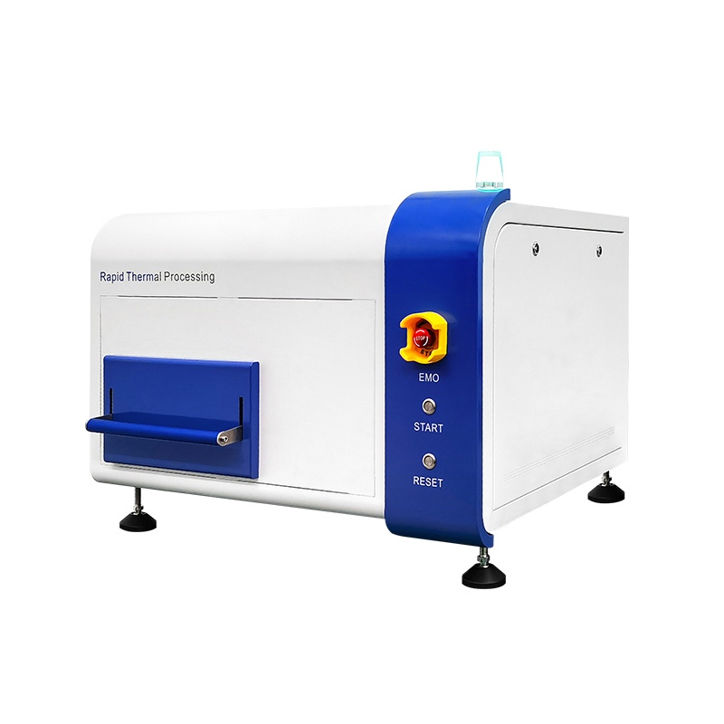
*Microwave plasma cleaning machine
Aiming at the semiconductor industry, it can meet the requirements of DB/WB, plasma treatment before molding and before underfill.
二. Application of plasma treatment in advanced packaging
In advanced packaging, plasma technology is mainly used in underfill process, bumping process, redistribution layer (RDL) technology, etc.
●Flip-Chip process
By flipping the chip on the substrate, solder balls or bumps are used instead of metal wires for connection, which has the
advantages of higher connection density and shorter interconnection distance.

*Image source: Internet, please delete if infringed
In order to improve the stability of flip-chip, filling glue is usually used to reinforce the chip and substrate after flip-chip, so as
to reduce the difference in thermal expansion coefficient between the chip and the substrate and improve the stability and
reliability of the package.
●Bumping process
The bumping process is widely used in advanced packages such as FC, WLP, CSP, and 3D. Bumps refer to protrusions with
metal conductive properties that grow on the surface of the chip and are directly or indirectly connected to the chip pad.

*Bumping process, source: Internet, please delete if infringed
In order to achieve better welding results, plasma is used for surface activation before welding to improve the wettability of the pad surface, thereby improving the welding firmness between the pad and the bump and improving the subsequent packaging quality.


 Home
Home